Type 3 Complex
Rf90953a.exe Reference disk for Type 3 Complexes
Rd9095a.exe Common Diagnostics for all 859x
/ 959x Systems
52G9619 1993 BIOS
Original Mitsubishi M5M27C201 PLCC32
192-101 IBM PS/2 Enhanced 486/50 Processor
Upgrade
Specifications
Memory supported, cache, features
Support for >1GB Disks as IML Drive
False ARTIC Diag Error
Type 3 Evergreen cpu upgrade that worked
"M"/ Upgrade 486DX 50 MHz 57F1597
Daughtercard
Why DX50 is on a
Daughtercard
Downlevel
Complex Incompatible with some Streamers
Daughtercard
Rework
Rework on Right
Rework
on Left
Base Board
Diagnostic LEDs
U27 Burning
"M"/
Upgrade 486DX 50 MHz 57F1597
FCC ID ANOIBM486B50 Sticker is 71G6207.
DX50 Base Board
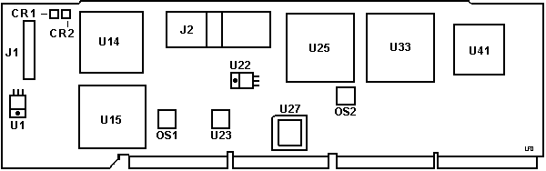
CR1, CR2 Diagnostic
LEDs
J1
Solder pads for 25 pin header
J2
Socket for Daughtercard
OS1
40.0000 MHz MCA Bus clock
OS2
22.1184 MHz Osc- Dunno.
U1,22 Voltage Regulators
U14
96F1920 Memory Data Buffer |
U15 96F1921
Memory Addr. Buffer
U23
87X0079
U25
10G7459ESD ???
U33
92F1477ESD ???
U27
41G9251 BIOS ('92)
52G9619 BIOS ('93)
U41
10G7808 DMA Controller (Type 2) |
U27 BIOS. Mitsubishi variant
of the 27C201, (256K x 8-bit.)
87X0079 What
is this? It's on all later complexes.
J1 Earlier versions had
a double pin-row connector at that place ... intended for the (or: one) precessor
of the Systems Management Adapter used on "high availability network servers".
Diagnostic
LEDs
The 50-MHz Type 3 complex in a 90/95 (submodel code 28 and 29),
has two LEDs; CR1 and CR2. During POST, CR1 comes on momentarily and CR2
stays off. If the LEDs work any other way, suspect that the processor board
is defective.
Use the LEDs to help differentiate between a processor board
or a system board failure. If you are instructed to replace one of the boards,
and the problem still exists, replace the other board (also reinstall the
first board). (Ed. Reports coming in
make me wonder about any of this. If the board passes diagnostics, and works
normally, do you really care about the LEDs?)
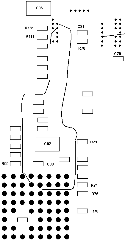
Daughtercard
71G6190
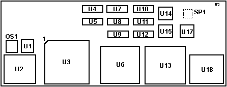
OS1 50 MHz
CPU Clock
SP1
71G6205
U1
87X0079
U2
78F1639 Address Buffer
U3
486DX-50 (5v) |
U4,5,7-12
L2 Cache
U6
96F1992 Data Buffer
U13,18 L2 Cache controller Set
U14,15,17 TI SN74BCT 2160-12FM
0 |
U13, U18 L2 Cache Controller
U4, U5, U7-U12 Toshiba TC55B329J-12
Why DX50 is
on Daughtercard
The DX50 is on the daughtercard because of the odd Intel cache
chipset. The chipset has limits on the distance it can be installed away
from the CPU. The only was to use the CPU and cache together was to place
them on a daughtercard.
Versions
Incompatible with Network Streamers
The downlevel processor card is identified by the lack of a
module in position SP1. This card may cause data loss or undetected change
in the:
Lanstreamer MC 16 PN 58G8999
Lanstreamer MC 32 PN 92F8941
Etherstreamer MC 32 PN 59G9081
Specifications
Memory
8/64MB parity or ECC same limits, PS/2 72-pin SIMM, Interleaved SIMMs ONLY.
All 64MB of memory are addressable by 32 bit DMA. SIMMs
must be installed in pairs of matched speed and size. Mixing Parity and ECC
is not allowed, not even if the pairs are matched.
Cache: 8kb L1, 256kb L2 cache
* 40 MB per second streaming
data transfer support.
* Error Checking and
Correcting (ECC) memory controller
* 256KB Level 2 memory cache (write-through) is standard.
* 20 MHz DMA; 32 bit DMA; DMA supports Subsystem Control Block.
* Faster bus arbitration (than Base 1) for busmaster performance.
* Enhanced
Dual Path Memory
* Subsystem
Control Block enabled
* Vital
Product Data support.
* Synchronous
Channel Check support
* Data
bus parity support
* A logging facility is provided (for ECC or system errors).
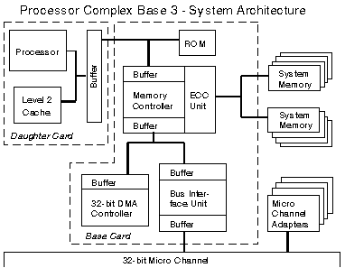
M Complex Block Diagram
Daughtercard
Rework
Dr. Jim sez: Documenting patch wire locations
is great, but remember that there are often foil cuts associated with them.
And you can't always see all of those. Ed. One can dream, can't
we?
I have seen one card with the older
BIOS 41G9251 ('92) that has NO rework. The three DX50 I have with the new
BIOS 52G9619 ('93) all have the rework. Why? Haven't a clue.
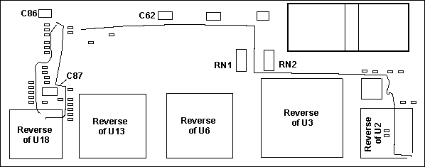
Daughtercard
Rework on Right
Daughtercard Rework
on Left
>1GB Drives as IML
The M complex supports >1GB drives as the IML source. No
complex BIOS upgrade is needed (or available). However, the SCSI controller
needs the enhanced SCSI BIOS of 92F2244 / 92F2245 to IML properly.
False ARTIC
diag error
SYMPTOM: When running diagnostics on the ARTIC Portmaster Adapter/A
in an 8590 or 8595 with the 486/50MHZ processor card installed, a false 14220,
E0DE error may occur.
PROBLEM ISOLATION AIDS: Check the date of the Portmaster Adapter/A
diagnostic file (DEV141.DGS) on the system reference diskette. Files dated
1-31-90 or earlier will exhibit the symptom.
FIX: Download updated Portmaster Adapter/A option diskette
Dead.
U27 Burning
Rick Ekblaw plays deep safety:
The M5M27C201JK is a 2 Megabit part, organized as 256K x 8,
with a 12V programming voltage. Logically, it's equivalent to other
2 Megabit EPROMs in the 27-class, such as the Intel/TI/AMD/Atmel 27C020 or
the Fujitsu/NEC/SGS/ST 27C2001 (see HERE, for example).
However, the DIP form factor was still in common use in this time frame,
and some of the PLCC varieties did not offer a windowed part (One-Time Programming
only).
So, the good news is that you could use almost any
2Mb PLCC32 EPROM or PROM that you can find to act as a replacement for the
M5M27C201JK as the BIOS chip in your M complexi (where it is only being read
by the system). For programming the EPROM/PROM, you have to choose
a part for which you have appropriate algorithms in your programmer, because
they vary.
> I was all set to install a power stacker 133/586
on my dx50 in the 9595-omt. I for some reason decided to RTFM while having
a cuppa. they say the powerstacker will not work with dx50. what cpu can
I use to juice up the dx50.?
Jim Shorney
Pay no attention to the manual. Set the multiplier
to x3, the cache jumper (if present) to write-through, and plug it in.
It will probably work fine.
9595 Main Page
|