|
Tandy 5000MC (250-6000)
mcmfm.exe - 22.3 kb - 09-17-93
- This file contains a microchannel MFM disk driver written for the IBM
Model 80, Tandy 5000, and other microchannel machines using an MFM controller.
The driver is for NetWare v3.0.
Information Files:
2410 Beep Codes
1727 Math Coprocessor
1723 Memory Upgrades (includes jumper
settings)
1728 Parallel Port
1725 Pinouts
1722 Settings
1724 Setup (describes the missing refdisk menus)
1721 Specifications
1726 Video Modes
22041 Detailed Parts List
22042 Detailed Parts List
22043 Detailed Parts List
Planar
Power
Plug Pinout
CPU Card
Memory Card
Exploded View
Main Logic
P/N 8899061
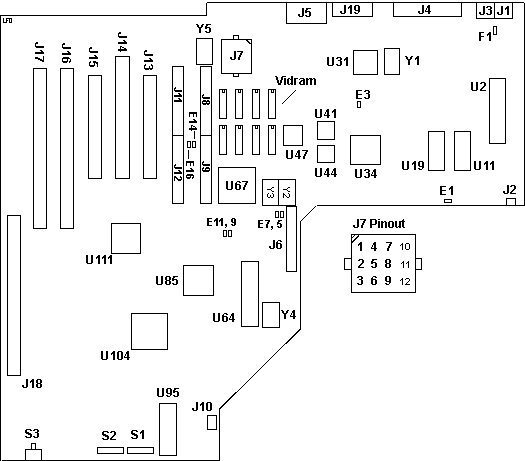
E1 CMOS Clear
E3,4 (do not use)
E5,6,7,8 (do not use)
E7,5
E11,9
E14,16
F1 1A (Canadian version only)
J1 Keyboard
J2 LED
J3 Mouse
J4 Parallel
J5 Video
J6 Floppy
J7 Power
J8,9 Memory Card 1
J10 Speaker
J11,12 Memory Card 2
J13,15 16 bit MCA slot
J14 16 bit MCA slot with AVE
J16,17 32 bit MCA slot
J18 CPU slot
J19 Serial
S1 Memory Card Defintion Switch
HERE |
S2 Memory Definition HERE
S3 Reset
U2 8742 Keyboard Controller
U11 DS1220Y 200nS (Non Vol RAM)
U19 DS1287A RTC (Non Vol RAM)
U31 NS16550A UART
U34 82306 LCS (Local Channel Support)
U41,44 8259A Interrupt Controller
1 and 2
U47 INMOS IMSG176 CLUT
U64 82072 FDC Supported
drives
U67 82706 VGA Video
Modes
U85 82309 ABC Address Bus Controller
U95 128k x 8 EPROM 27C100K-15
U104 82307 DMA and CACP Controller
U111 82308 BCS Bus Control System
(MCA)
Vidram 64k x 4 120nS
Y1 1.8432MHz osc UART
Y2 25.175MHz osc Video
Y3 28.322MHz osc Video
Y4 24MHz osc FDC
Y5 14.31818MHz osc Base clk for
many things.
0 |
As of 19 Jan 06, I have to clear up
the memory jumpers. They can be placed across two headers, not just one.
So any pair of jumpers on this outline can have more than four combinations...
My brain hurts...
J7 Power Pinout

1,2,4,5 +5V
3 +12V
6,7,8,9 Gnd |
10 -5V
11 -12V
12 Pwrgood |
Floppy Controller
Supports 360K, 1.2M, 720K and 1.44MB drives. Transfer
rates are 250K or 500K, so it cannot support 2.88MB. Don't try it.
Parallel Port
Parallel port follows IBM conventions, IRQ7 only and swapped LPT1 and
LPT2. It can be set up as Compatible (ouptut only) or Extended mode (bidirectional).
LPT Data Status
Control
1 03BCh 03BDh
03BEh
2 0378h 0379h
037Ah
3 0278h 0279h
027Ah
S1 Memory Card Definition
Switch (also P103)
Now to figure out which switch is what... Looks as
if these bits have some sort of logical operation performed on them, there
is no direct correlation between bits 3-2 and 1-0 that is apparent.
I did find S1, but it is not labled, and it feeds some logic
chips.
Bit 7 - 2MB/8MB Card installed. 0 = 8MB card
Bit 4-6 - Reserved = 1
Bits 3-2 Memory Card in second connector
Bit 3 Bit2
0
0 Invalid
1
0 Memory card in second connector
1
1 No card in connector 2
Bits 1-0 Memory Card in first connector
Bit 1 Bit0
0
0 Invalid
1
0 Memory card in first connector
1
1 Invalid (of course, mem1 is always used!)
S2 Memory
Definition Switch
Not seen a real name, so I guessed.
Pin Name
Description
1 2/4 Banks
One card ON, Two cards OFF
2 LIM Enable Lotus-Intel-Microsoft
extended memory LEAVE OFF
3 Non-Page Mode OFF use paged memory
ON disable paged memory
4 Fast Mode
What? LEAVE ON
5 N/C
What? LEAVE OFF
6 N/C
7 N/C
8 256K/1MB
256K simms ON, 1MB simms OFF
My guesses for valid configurations. It looks that the
memory controller cannot handle mixed simms, unlike our beloved PS/2s.
As the memory is interleaved, all eight sockets on each card need to be
filled.
2MB
4MB 8MB 16MB
Card1 256k 256k 1MB
1MB
Card2 No 256k
No 1MB
Banks 2 4
2 4
CPU Board Rev
A. P/N 8709839
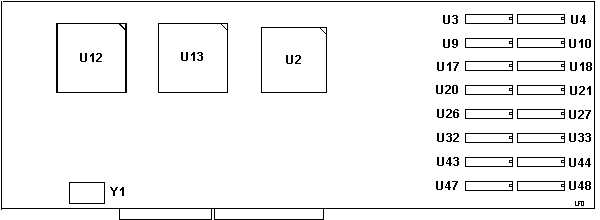
U2 80387DX-20 Math Co-pro
U12 80386DX-20 CPU
U13 82385-20 Cache Controller |
U3 thru 48
4k x 4 25nS SRAM
Y1 40MHz osc
0 |
L2 cache is organized as two banks (A and B) of 4k double words.
Cache hits, DRAM or bank, returned with 0 wait states.
Cache miss with page hit is returned with 2 wait states.
Cache miss with page miss is returned with 4 wait states.
Memory PCB Rev B
P/N
8899065 25-6030
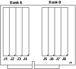
256K SIMMS
256K X 9 SIMM chips at 80 or 100nS
1MB SIMMS
1 MB x 9 SIMM chips at 60, 80 or 100nS
Jumper and switch settings
Battery Replacement:
MX-1560: (U11) CMS Battery Clock Chip
MX-1561: (U19) DS1287A REAL TIME
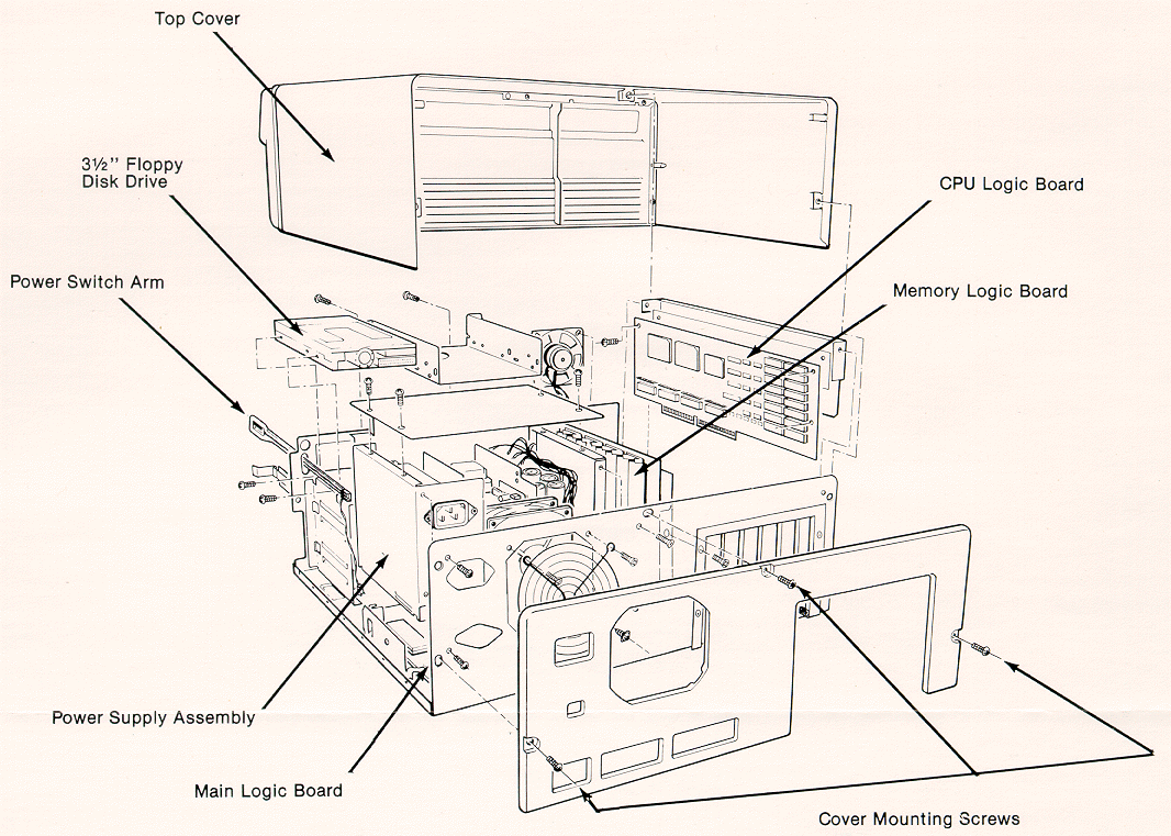
Exploded View
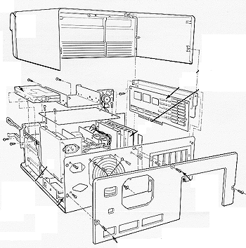
For a higher detail version, click HERE
9595 Main Page
|